Succeeding in observing in real time how crystalline materials break with the use of electron microscope and microdevice
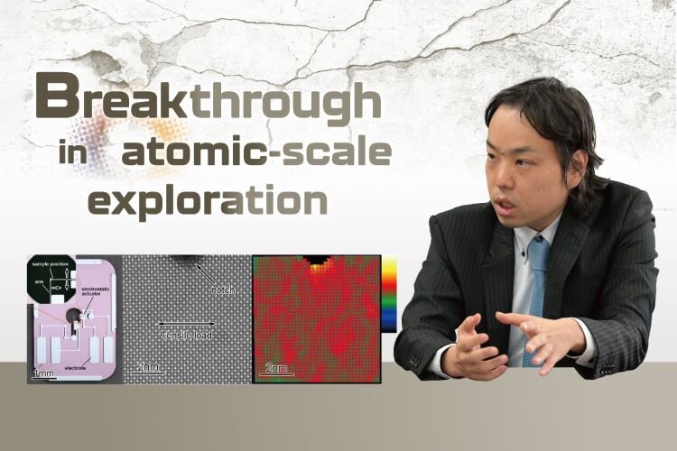
Scientists have long grappled with the challenge of observing how industrial materials deform and break at an atomic scale. This was seen as daunting, if not impossible, leading many researchers to focus on developing algorithms for simulating failure mechanisms. However, Associate Professor Eita Tochigi of UTokyo-IIS has astonished his peers by achieving real-time observations of how crystalline materials deform and break at an atomic scale. He utilized Transmission Electron Microscopy (TEM) in conjunction with a Micro Electro Mechanical System (MEMS).
An accidental TEM researcher meets MEMS expert
As a fourth-year student at Hokkaido University, Tochigi joined a laboratory dedicated to transmission electron microscope (TEM) research, but without excitement, because the field was not his first choice. He gradually developed an interest in observing how things deform and break, eventually advancing to the University of Tokyo's Graduate School of Engineering, where he earned a doctoral degree in material engineering in 2011.
After a two-year stint as a postdoctoral researcher at the Lawrence Berkeley National Laboratory in the United States, he served as an assistant professor at the UTokyo graduate school, researching TEM at the laboratory of Professor Yuichi Ikuhara from 2013 to 2021. It was during this period that he had a fateful encounter. "I met Professor Hiroyuki Fujita, a renowned MEMS professional affiliated with IIS (before his retirement in 2018)," Tochigi said. "Having only researched TEM, I didn't know anything about MEMS."
The collaboration between the Ikuhara and Fujita research groups, coming from different fields, ultimately resolved the thorny issue of placing and controlling samples in a tiny holder (measuring a few millimeters) inside the TEM apparatus when a load is applied. This collaboration led to the development of the so-called in situ mechanical test system for atomic-resolution transmission electron microscopy, driven and controlled by a new device using MEMS technology.
"It took five to six years to develop this technology, a process that involved refining the MEMS device and figuring out the optimal method for placing samples in the microscope," Tochigi explained. He highlighted the challenges faced in making the microscope -- a technology developed in the 1930s -- suitable for achieving real-time, direct observation of atomic behavior.
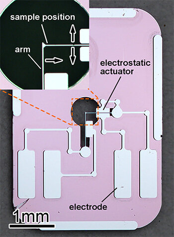
MEMS loading device for TEM.
'Something weird is happening'
One day, Tochigi was observing a ceramic material with the just-completed advanced scanning TEM -- a device that transmits a beam of electrons through the sample, collecting resulting signals underneath to create images of its crystalline structures. As he applied pressure with an indenter tip to the sample, he was astonished. "At first, I thought I observed a weird phenomenon," he said, describing how the ceramic material fractured on an atomic scale.
"The phenomenon was totally unexpected, because it differed from what past simulations showed," he recalled. This marked the first instance of any researcher observing a fracture on an atomic scale. Tochigi and other researchers later confirmed that the arrangement of molecules within ceramic grains influences the way a fracture propagates.
But for Tochigi, witnessing the phenomenon at an atomic scale is not the end goal; rather, it marks the beginning of elucidating the mechanisms behind crystalline defects such as dislocation and deformation twinning in crystal lattices. Dislocation refers to a crystal defect involving an abrupt change in the arrangement of atoms within a crystal structure, while deformation twinning involves the intergrowth of two or more crystal grains, creating either a reflected image of each other or rotation between them.
Tochigi can now produce a video demonstrating how crystal defects occur using his scanning TEM system, departing from the still images most scientists are familiar with. The maximum resolution of the system allows observation of an atom as small as 40 picometers.
"While I might have sounded as if I held a monopoly over the technique, my intention is to encourage many researchers to take an interest in direct atomic-scale observation and stimulate greater research in this field," Tochigi said.
Exploring real-world uses for jet engine blades
Tochigi's project is fundamentally oriented towards basic research, yet it holds the potential for practical applications in designing and manufacturing more robust industrial materials in the future. Crystalline materials, known for their robustness and high heat resistance, are ideal for various applications, including electronic devices, light-emitting elements, optical components, and energy conversion elements, as well as structural materials. For instance, ceramic materials find applications in both small devices like smartphones and large structural materials for buildings.
Ensuring the development of robust and safe materials is crucial, especially in applications like jet engine turbine blades. These blades often utilize nickel-based superalloys coated with ceramics. Exposed to stresses during engine operations, such as rapid heating and cooling, damaged turbine blades can lead to catastrophic engine failure.
To prevent such failures and create more robust materials, understanding the atomic-scale mechanism of ceramic sintering is vital, Tochigi said. Ceramic materials are composed of powders that coalesce during the process of sintering, forming grain boundaries. The movement of these grain boundaries influences the size of the grain, and is closely related to the material's strength and functions. In 2022, Tochigi and his colleagues at UTokyo published an article on their research results in the British journal Nature Communications.
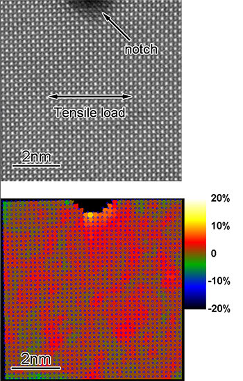
(Upper) Scanning TEM image of SrTiO3 single crystal under loading.
(Bottom) Strain map (exx). [1]
[1]E. Tochigi, T. Sato, N. Shibata, H. Fujita, Y. Ikuhara, Microsc. Microanal. 26, S2, 1838-1840 (2020).
Expanding the research horizons with TEM
As an immediate goal, Tochigi wants to refine direct atomic-scale observation technology, making it applicable to various specimens, such as polymers.
"Currently, TEM faces limitations in observing organic and polymer materials," Tochigi explained. "If we can achieve atomic-scale observation of polymers, interest in our technology will undoubtedly increase. I hope to collaborate with other researchers to advance my research."
Short Dialogue
Associate Professor Minami(→Sensing the unseen world [UTokyo-IIS Bulletin Vol.13] ):
I am struck by how inward-looking Japanese students can be. When I was a postdoc and a research assistant professor in the US, the lab had many international students and researchers. When I established my own lab at UTokyo-IIS, I was determined to make it globally oriented, and I succeeded in attracting international researchers.
Associate Professor Tochigi:
I am very concerned about attracting students and researchers from around the world. A failure in this regard impedes international exchange in the academic field. I am also worried about Japanese students, many of whom regard research jobs as unattractive. As a young researcher, my mission is to conduct research that appeals to young people.
Minami:
Yes, as young researchers, we have to bring innovations to Japan, which seems to have rested on its past spectacular achievements for too long.
Reference
Jiake Wei, Bin Feng, Eita Tochigi, Naoya Shibata, Yuichi Ikuta, "Direct imaging of the disconnection climb mediated point defects absorption by a grain boundary", Nature Communications (2022), DOI:10.1038/s41467-022-29162-2